 | –≠–ª–µ–∫—Ç—Ä–æ–Ω–Ω—ã–π –∫–æ–º–ø–æ–Ω–µ–Ω—Ç: BAV99RWT1 | –°–∫–∞—á–∞—Ç—å:  PDF PDF  ZIP ZIP |
©
Semiconductor Components Industries, LLC, 2005
January, 2005 - Rev. 4
1
Publication Order Number:
BAV99WT1/D
BAV99WT1, BAV99RWT1
Preferred Devices
Dual Series Switching
Diodes
The BAV99WT1 is a smaller package, equivalent to the BAV99LT1.
Features
∑
Pb-Free Packages are Available
Suggested Applications
∑
ESD Protection
∑
Polarity Reversal Protection
∑
Data Line Protection
∑
Inductive Load Protection
∑
Steering Logic
MAXIMUM RATINGS
(Each Diode)
Rating
Symbol
Value
Unit
Reverse Voltage
V
R
70
Vdc
Forward Current
I
F
215
mAdc
Peak Forward Surge Current
I
FM(surge)
500
mAdc
Repetitive Peak Reverse Voltage
V
RRM
70
V
Average Rectified Forward Current
(Note 1)
(averaged over any 20 ms period)
I
F(AV)
715
mA
Repetitive Peak Forward Current
I
FRM
450
mA
Non-Repetitive Peak Forward Current
t = 1.0
m
s
t = 1.0 ms
t = 1.0 S
I
FSM
2.0
1.0
0.5
A
Maximum ratings are those values beyond which device damage can occur.
Maximum ratings applied to the device are individual stress limit values (not
normal operating conditions) and are not valid simultaneously. If these limits are
exceeded, device functional operation is not implied, damage may occur and
reliability may be affected.
1. FR-5 = 1.0
0.75
0.062 in.
Device
Package
Shipping
ORDERING INFORMATION
BAV99WT1
SC-70
3000/Tape & Reel
Preferred devices are recommended choices for future use
and best overall value.
BAV99RWT1
SC-70
CASE 419, STYLE 10
BAV99WT1
SC-70
CASE 419, STYLE 9
3
CATHODE/ANODE
ANODE
1
CATHODE
2
1
2
3
CATHODE/ANODE
CATHODE
ANODE
BAV99RWT1
SC-70
3000/Tape & Reel
1
2
3
MARKING
DIAGRAM
A7 = BAV99WT1
F7 = BAV99RWT1
D = Date Code
x7....D
SC-70
CASE 419
BAV99RWT1G
SC-70
(Pb-Free)
3000/Tape & Reel
For information on tape and reel specifications,
including part orientation and tape sizes, please
refer to our Tape and Reel Packaging Specifications
Brochure, BRD8011/D.
BAV99WT1G
SC-70
(Pb-Free)
3000/Tape & Reel
http://onsemi.com
BAV99WT1, BAV99RWT1
http://onsemi.com
2
THERMAL CHARACTERISTICS
Characteristic
Symbol
Max
Unit
Total Device Dissipation FR-5 Board, (Note 1) T
A
= 25
∞
C
Derate above 25
∞
C
P
D
200
1.6
mW
mW/
∞
C
Thermal Resistance Junction-to-Ambient
R
q
JA
625
∞
C/W
Total Device Dissipation Alumina Substrate, (Note 2) T
A
= 25
∞
C
Derate above 25
∞
C
P
D
300
2.4
mW
mW/
∞
C
Thermal Resistance Junction-to-Ambient
R
q
JA
417
∞
C/W
Junction and Storage Temperature
T
J
, T
stg
- 65 to +150
∞
C
ELECTRICAL CHARACTERISTICS
(T
A
= 25
∞
C unless otherwise noted) (Each Diode)
Characteristic
Symbol
Min
Max
Unit
OFF CHARACTERISTICS
Reverse Breakdown Voltage (I
(BR)
= 100
m
A)
V
(BR)
70
-
Vdc
Reverse Voltage Leakage Current
(V
R
= 70 Vdc)
(V
R
= 25 Vdc, T
J
= 150
∞
C)
(V
R
= 70 Vdc, T
J
= 150
∞
C)
I
R
-
-
-
2.5
30
50
m
Adc
Diode Capacitance
(V
R
= 0, f = 1.0 MHz)
C
D
-
1.5
pF
Forward Voltage
(I
F
= 1.0 mAdc)
(I
F
= 10 mAdc)
(I
F
= 50 mAdc)
(I
F
= 150 mAdc)
V
F
-
-
-
-
715
855
1000
1250
mVdc
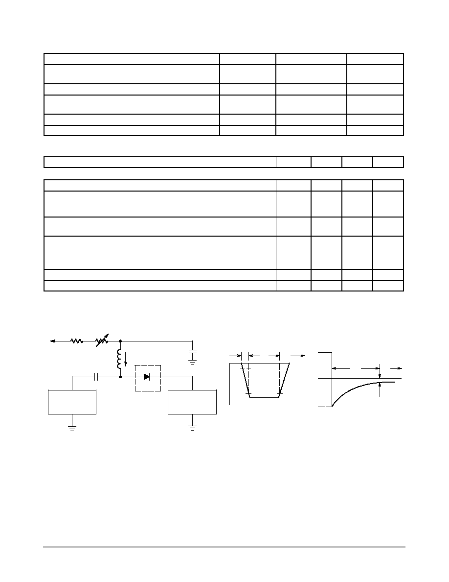
Reverse Recovery Time (I
F
= I
R
= 10 mAdc, i
R(REC)
= 1.0 mAdc) (Figure 1) R
L
= 100
W
t
rr
-
6.0
ns
Forward Recovery Voltage (I
F
= 10 mA, t
r
= 20 ns)
V
FR
-
1.75
V
1. FR-5 = 1.0
0.75
0.062 in.
2. Alumina = 0.4
0.3
0.024 in. 99.5% alumina.
Notes: (a) A 2.0 k
W
variable resistor adjusted for a Forward Current (I
F
) of 10 mA.
Notes:
(b) Input pulse is adjusted so I
R(peak)
is equal to 10 mA.
Notes:
(c) t
p
ª t
rr
+10 V
2 k
820
W
0.1 mF
DUT
V
R
100 mH
0.1 mF
50 W OUTPUT
PULSE
GENERATOR
50 W INPUT
SAMPLING
OSCILLOSCOPE
t
r
t
p
t
10%
90%
I
F
I
R
t
rr
t
i
R(REC)
= 1 mA
OUTPUT PULSE
(I
F
= I
R
= 10 mA; measured
at i
R(REC)
= 1 mA)
I
F
INPUT SIGNAL
Figure 1. Recovery Time Equivalent Test Circuit
BAV99WT1, BAV99RWT1
http://onsemi.com
3
CURVES APPLICABLE TO EACH DIODE
I R
, REVERSE CURRENT
(A)
µ
100
0.2
0.4
V
F
, FORWARD VOLTAGE (VOLTS)
0.6
0.8
1.0
1.2
10
1.0
0.1
T
A
= 85
∞
C
10
0
V
R
, REVERSE VOLTAGE (VOLTS)
1.0
0.1
0.01
0.001
10
20
30
40
50
0.68
0
V
R
, REVERSE VOLTAGE (VOLTS)
0.64
0.60
0.56
0.52
C
D
, DIODE CAP
ACIT
ANCE (pF)
2
4
6
8
I F
, FOR
W
ARD CURRENT
(mA)
T
A
= 25
∞
C
T
A
= -40
∞
C
T
A
= 150
∞
C
T
A
= 125
∞
C
T
A
= 85
∞
C
T
A
= 55
∞
C
T
A
= 25
∞
C
Figure 2. Forward Voltage
Figure 3. Leakage Current
Figure 4. Capacitance
BAV99WT1, BAV99RWT1
http://onsemi.com
4
PACKAGE DIMENSIONS
SC-70 (SOT-323)
CASE 419-04
ISSUE L
C
N
A
L
D
G
S
B
H
J
K
3
1
2
NOTES:
1. DIMENSIONING AND TOLERANCING PER ANSI
Y14.5M, 1982.
2. CONTROLLING DIMENSION: INCH.
DIM
MIN
MAX
MIN
MAX
MILLIMETERS
INCHES
A
0.071
0.087
1.80
2.20
B
0.045
0.053
1.15
1.35
C
0.032
0.040
0.80
1.00
D
0.012
0.016
0.30
0.40
G
0.047
0.055
1.20
1.40
H
0.000
0.004
0.00
0.10
J
0.004
0.010
0.10
0.25
K
0.017 REF
0.425 REF
L
0.026 BSC
0.650 BSC
N
0.028 REF
0.700 REF
S
0.079
0.095
2.00
2.40
0.05 (0.002)
*For additional information on our Pb-Free strategy and soldering
details, please download the ON Semiconductor Soldering and
Mounting Techniques Reference Manual, SOLDERRM/D.
SOLDERING FOOTPRINT*
1.9
0.075
0.65
0.025
0.65
0.025
0.9
0.035
0.7
0.028
mm
inches
SCALE 10:1
STYLE 9:
PIN 1. ANODE
2. CATHODE
3. CATHODE-ANODE
STYLE 10:
PIN 1. CATHODE
2. ANODE
3. ANODE-CATHODE
ON Semiconductor and are registered trademarks of Semiconductor Components Industries, LLC (SCILLC). SCILLC reserves the right to make changes without further notice
to any products herein. SCILLC makes no warranty, representation or guarantee regarding the suitability of its products for any particular purpose, nor does SCILLC assume any liability
arising out of the application or use of any product or circuit, and specifically disclaims any and all liability, including without limitation special, consequential or incidental damages.
"Typical" parameters which may be provided in SCILLC data sheets and/or specifications can and do vary in different applications and actual performance may vary over time. All
operating parameters, including "Typicals" must be validated for each customer application by customer's technical experts. SCILLC does not convey any license under its patent rights
nor the rights of others. SCILLC products are not designed, intended, or authorized for use as components in systems intended for surgical implant into the body, or other applications
intended to support or sustain life, or for any other application in which the failure of the SCILLC product could create a situation where personal injury or death may occur. Should
Buyer purchase or use SCILLC products for any such unintended or unauthorized application, Buyer shall indemnify and hold SCILLC and its officers, employees, subsidiaries, affiliates,
and distributors harmless against all claims, costs, damages, and expenses, and reasonable attorney fees arising out of, directly or indirectly, any claim of personal injury or death
associated with such unintended or unauthorized use, even if such claim alleges that SCILLC was negligent regarding the design or manufacture of the part. SCILLC is an Equal
Opportunity/Affirmative Action Employer. This literature is subject to all applicable copyright laws and is not for resale in any manner.
PUBLICATION ORDERING INFORMATION
N. American Technical Support: 800-282-9855 Toll Free
USA/Canada
Japan: ON Semiconductor, Japan Customer Focus Center
2-9-1 Kamimeguro, Meguro-ku, Tokyo, Japan 153-0051
Phone: 81-3-5773-3850
BAV99WT1/D
LITERATURE FULFILLMENT:
Literature Distribution Center for ON Semiconductor
P.O. Box 61312, Phoenix, Arizona 85082-1312 USA
Phone: 480-829-7710 or 800-344-3860 Toll Free USA/Canada
Fax: 480-829-7709 or 800-344-3867 Toll Free USA/Canada
Email: orderlit@onsemi.com
ON Semiconductor Website: http://onsemi.com
Order Literature: http://www.onsemi.com/litorder
For additional information, please contact your
local Sales Representative.